HDI PCB
Name: HDI-PCB
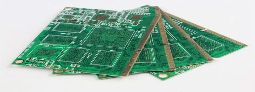
Composition: It is a circuit board with relatively high circuit distribution density using micro-blind buried hole technology. The HDI board has an inner layer circuit and an outer layer circuit, and then uses processes such as drilling and metallization in the hole to realize the internal connection of each layer of circuits
 Features:
✿ Thin and high-efficiency: Higher layers and thinner lines are used to make the entire circuit board compact and thin. It not only helps to reduce the volume and weight of products, improves portability and user experience, but also reduces production costs and energy consumption.
✿ Signal transmission performance: Due to its high-density wiring method and optimized structural design, HDI rigid-flex board can provide a more stable and high-speed signal transmission channel.
✿ Good electromagnetic compatibility (EMC) & thermal management performance: through reasonable layout and material selection, HDI rigid-flex board can effectively suppress electromagnetic interference and heat accumulation, protect electronic components from the external environment, and ensure Stable operation and long-term reliability of equipment.
Process: material cutting, inner layer dry film, blackening and browning, blackening and browning, drilling blind and buried holes, sinking copper and thickening copper, etc.
The difference between HDI and PCB
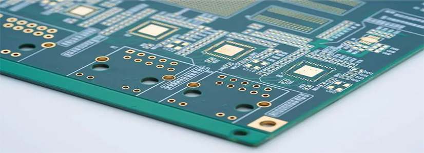
✿ Wiring density: HDI board has higher wiring density than ordinary PCB. Using blind hole and buried hole technology, HDI boards can realize more signal lines in a smaller size, providing higher wiring density and more complex circuit design.
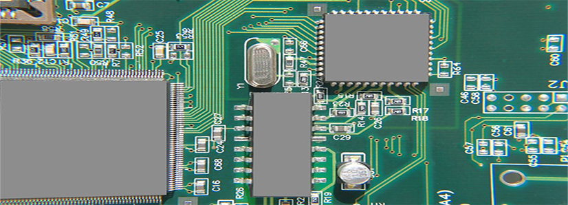
✿ Multi-layer structure: HDI boards usually adopt a multi-layer structure, including more than 4 layers. The multi-layer structure provides more signal layers, power layers and ground layers to support complex signal transmission and circuit connections.
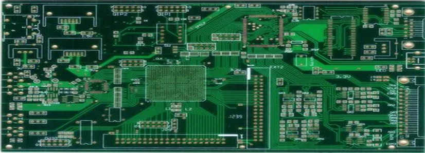
✿ Small size: Due to the advantages of high-density wiring and multi-layer structure, HDI boards can achieve smaller sizes than ordinary PCBs. This makes HDI boards more suitable for applications requiring compact packaging and space constraints.
✿ High-precision manufacturing: The manufacturing process of HDI boards requires higher-precision process control and advanced manufacturing equipment. For example, advanced technologies such as laser drilling and light painting technology are used to ensure accurate hole positions and detailed circuit patterns.
Applications: mobile phones, computers, network communications, automotive electronics and other fields.
none
Composition: It is a circuit board with relatively high circuit distribution density using micro-blind buried hole technology. The HDI board has an inner layer circuit and an outer layer circuit, and then uses processes such as drilling and metallization in the hole to realize the internal connection of each layer of circuits
✿ Thin and high-efficiency: Higher layers and thinner lines are used to make the entire circuit board compact and thin. It not only helps to reduce the volume and weight of products, improves portability and user experience, but also reduces production costs and energy consumption.
✿ Signal transmission performance: Due to its high-density wiring method and optimized structural design, HDI rigid-flex board can provide a more stable and high-speed signal transmission channel.
✿ Good electromagnetic compatibility (EMC) & thermal management performance: through reasonable layout and material selection, HDI rigid-flex board can effectively suppress electromagnetic interference and heat accumulation, protect electronic components from the external environment, and ensure Stable operation and long-term reliability of equipment.
Process: material cutting, inner layer dry film, blackening and browning, blackening and browning, drilling blind and buried holes, sinking copper and thickening copper, etc.
The difference between HDI and PCB
✿ Wiring density: HDI board has higher wiring density than ordinary PCB. Using blind hole and buried hole technology, HDI boards can realize more signal lines in a smaller size, providing higher wiring density and more complex circuit design.
✿ Multi-layer structure: HDI boards usually adopt a multi-layer structure, including more than 4 layers. The multi-layer structure provides more signal layers, power layers and ground layers to support complex signal transmission and circuit connections.
✿ Small size: Due to the advantages of high-density wiring and multi-layer structure, HDI boards can achieve smaller sizes than ordinary PCBs. This makes HDI boards more suitable for applications requiring compact packaging and space constraints.
✿ High-precision manufacturing: The manufacturing process of HDI boards requires higher-precision process control and advanced manufacturing equipment. For example, advanced technologies such as laser drilling and light painting technology are used to ensure accurate hole positions and detailed circuit patterns.
Applications: mobile phones, computers, network communications, automotive electronics and other fields.